
Analog can Scale. Here's how.
From a transistor to an MNIST accelerator, let's build up to see how an analog computing system would borrow the right abstractions to push the frontier of possible.

When I posted my last article, it got both positive reception and lots of classic confusion/questions about the things I was saying. Paraphrasing roughly, they were “what do you mean analog programming is novel, don’t we have trimming?” Or “that analog stuff is cool and all, but it really doesn’t scale” or “what about device variation? (mismatch)”. It was then I understandably realized I had a lot more explaining to do and it’s on me to be clearer about what’s going on at the lowest levels of our computing devices. Even members of niche forums dedicated to adjacent topics may not be aware of how the claims I was making about analog being so great mapped to the research papers that were linked. So, in this article, I’m going to walk through the stack. Starting from a simple transistor and its physics all the way to a system benchmark of an analog vs digital implementation.
What is a transistor?
It is a device with three or four terminals whose basic operation is to act like a valve for the flow of current between two terminals. More technically, using a “gate” or “base” pin, the amount of charge carriers (electrons or holes) moving between two other pins are modulated. A very simple analogy (which has flaws we will get to) is a tap. When you turn it “on” water flows and you can adjust the rate of water till the maximum throughput is flowing. There are two main types of transistors to consider: Bipolar Junction Transistors (BJTs) and Metal Oxide Semiconductor Field Effect Transistors (MOSFETs) but far more types exist. There is so much interesting history about how they stemmed from vacuum tubes and Field Effect Transistors were invented first but the BJT gained adoption before MOSFETs came to dominate most use cases today. But we have stuff to get through so maybe we’ll save history for another time.
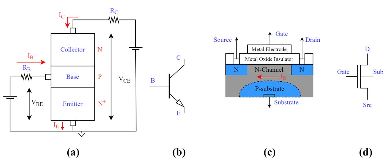
Figure 1: (a) Cross section of a BJT (b) Symbol of a BJT (c) Cross section of a MOSFET (d) Symbol of a MOSFET
While the BJT still has many uses in production chips today, the MOSFET will be the focus of our discussions due to its wider availability in process nodes from semiconductor manufacturers and the fundamental fact that floating gates can exist in a MOSFET because charge is stored at the gate. A BJT would see that stored charge flow through one of its terminals (see Figure 1 for BJT vs MOSFET cross section). Quick aside on the MOSFET symbol: Even though it’s a 4-terminal device, the substrate voltage is usually held constant and is often not shown in symbols.
Digital vs Analog View
Focusing on the MOSFET we can circle back to one flaw of the valve analogy. With a water valve, the water can be completely turned off when the valve is closed but in MOSFETs you could still have some electrons flowing through the channel even when you have applied the proper voltage to turn the device “off”. In fact, this binary view of a transistor is one of the interesting fundamental divides between a digital and analog view of the same transistor current.
Take one of the most basic curves for understanding a transistor: a gate voltage sweep as caricatured in Figure 2. This is a circuit experiment for say an N-type MOSFET where you apply a fixed higher potential to the drain, apply ground to the substrate terminal, slowly raise the gate voltage from ground to the fixed potential and measure the current coming out of the source.
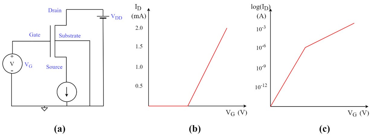
Figure 2:(a) Gate sweep circuit setup (b) Linear view of current (c) Logarithmic view of current
A digital or binary view of the transistor is to say up till the mid-point (aka threshold voltage) the transistor is off and when the current is maximum the FET is on (Fig 2b). An analog or continuous view would be to take the logarithm of the current (Fig 2c) and we see even at the lowest voltage there is a corresponding change in the output current with far more intermediate states (10-12 to 10-3 is 9 orders of magnitude or 1,000,000,000 levels). It is important to pause to acknowledge the major tradeoffs between these two views. Neither is wrong but with a binary view there are only two states to keep track of so signals are easily recovered. With a continuous view, far more information can be encoded across those levels, but more effort is paid to processing, storing and recovering signals. However, this basic distinction starts to underscore how much more efficient analog processing can be. In the previous article, we showed how many fewer transistors analog circuits could use for similar operations. Now we see there’s much lower current levels analog circuits can operate at.
What is a Floating Gate FET?
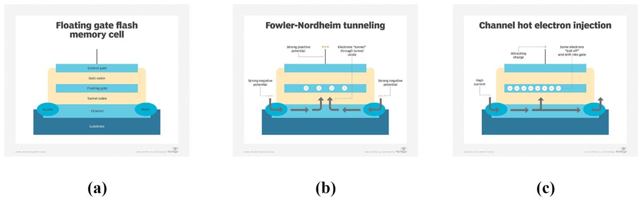
Figure 3: (a) Flash memory cell cross-section (b) FN tunneling operation (c) Hot electron injection operation. Source: Tech Target. https://www.techtarget.com/searchstorage/definition/floating-gate
At its simplest, a floating gate FET is a MOSFET with extra capacitance at the gate terminal capable of storing charge (Figure 3a). The mechanisms for storing or removing said charge at the isolated gate capacitance include Fowler Nordheim tunneling (Figure 3b) and Hot electron injection (Figure 3c). Why would we want to store charge at the gate? Traditionally this has been a way to give computers longer term memory. Specifically, “non-volatile” memory in SSDs and SD cards which is separate from volatile, short-term memory like SRAM or DRAM. Non-volatile here means that when voltage is removed from the circuit (powered down) the value is still retained.
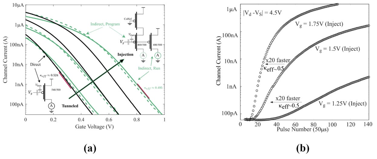
Figure 4: (a) Gate sweep and IV curve data from the 65nm paper showing FG std cell. (b) Targeted precise programming and time to reach a particular current. Both figures from this paper.
The little transistor that could, FGs can do more than just hold data. Researchers have long since shown they can perform useful computation. So how does it apply to the digital vs analog computing divide? Or help analog circuits scale? It does so by allowing the effective threshold voltage to shift, or be programmed, after manufacturing. The “shifting” of the gate voltage sweep (colloquially know as IV curve) can be seen in Fig 4a while the programming to a target current in seen in 4b. Both figures are taken from this research paper. As a primitive it allows analog circuit designers to fight mismatch, to change the value of a bias current and generally to create abstractions previously not seen in the analog world. Those abstractions we will have to come back to.
One last thing on FGs, in the last article I talked about analog computing and crossbars so its useful here to compare the FG FET to other potential technologies as crossbar elements. The colloquial system-level metrics used by the industry are power, performance, area and (when you’re the one paying) cost. But for crossbar elements the following metrics are salient: precision, drift/refresh, device isolation, current draw, fabrication maturity. Taking each in turn, we can compare FGs to memristive (ReRAM), digital (SRAM) and Magnetic Tunneling Junctions (MTJs). Precision refers to the number of reliable states that can be programmed and outside of digital, FGs have the highest precision of these technologies. This can result in a larger search space for training neural networks and in an energy constrained environment the ability to trade precision for fewer parameters can provide real savings. Even with digital having higher precision we can then analyze the current draw. As we have seen from counting in the previous article or IV curves above, the increase in precision of digital circuits translates to orders of magnitude more power consumption due to more transistors and more current per transistor. Furthermore, because FGs can operate in the subthreshold regime it puts them in a lower power range than the other devices. Next is programming drift, devices like ReRAM need to be periodically refreshed while FGs have 10-year retention lifetimes when high-quality insulators are provided. Next, we have device isolation which refers to the ability to target and program a single device in a crossbar. The three terminals in a transistor allow only a selected device to be active while others are driven into a deep depletion state. The two terminal devices like MTJs and ReRAM must deal with sneak currents. And finally, the fabrication maturity and research on FGs have shown how to create them without any extra mask steps. This fundamentally separates FGs as a scalable technology today vs others which need back-end steps to be integrated like MTJs, ReRAM, PCM etc.
Conventional approaches to analog and digital circuit design
I would say we’ve gone knee-deep into transistor level discussions so far but before we get lost down the rabbit hole, lets pull back for a broad view of what those transistors are being used for. Specifically, I’d like to broadly describe both topics to highlight similarities and differences to the analog computing approach.
Analog Circuit Design
To create or select analog circuits for an application there are a few different schools of thought. The first is how a lot of designers primarily rely on their magical “analog designer’s intuition” to guide them. This comes from years of experience and a mental library/familiarity with many standard topologies. So, a lot more time is spent analyzing and sizing the transistors within a topology to hit the specification. While I don’t have exact numbers, my estimation from seeing the process across industry and academia is that true novel circuit design is generally rare. Which counterintuitively is a good thing. When the circuit really needs work for a known application and with how expensive chip design can be it makes sense to be quite conservative with qualifying a new topology. Continuing with approaches there’s the gm/ID method that’s become more popular in the recent decade I’d say. This involves generating a lot of tables for transistor sizes in a particular process node and working through standard equations to connect the transconductance (gm) of a transistor to a specification like amplifier gain/bandwidth. One thing I really like about this approach is it tries to systematize some of that magic designer’s intuition by drawing very direct connection between data, equations and tradeoffs for a target metric. There are also various independent approaches like leaning on the EKV model for design in weak and moderate inversion. Or primarily turning circuits into their small signal model and using the square law equations to cancel the lower priority terms in the strong inversion region of the transistor. Ultimately, analog circuit design is much less unified than digital design which can make it feel more artistic.
Trimming vs Programmability
Across the approaches above, none of them are geared towards having any specifications change after chip fabrication. This is a good time to clarify the difference between trimming and “programming” as I mean it. Trimming is the act of introducing external elements like a resistor to finely adjust current values (which translate into specification like gain, bandwidth etc if placed around the right transistor) to deal with mismatch from manufacturing. Additionally, some digital circuits can also be placed nearby to store value for the new trimmed state. The major hurdle of this approach is if you know anything about chip design you know that resistors of any decent value on chip are massive! I’m talking 10 – 100x the transistor size for one resistor. So is synthesizing a digital circuit to place nearby. Not to mention that a clocked, high-speed digital circuit also introduces noise and interference to your analog circuit if you’re not careful. Generally, this means trimming is better for specialized, bespoke circuits. i.e. making 1-5 Op-amps on die to sell. Or creating ADCs with maybe a few channels. That is how the field of chip design has historically viewed analog circuits. A niche part of the chip that can do some specialized operation, but whose job is mainly to sanitize some input then quickly ferry things into the digital domain for computing. I’d be remiss if I didn’t point out there are analog systems that are “larger in scale” like phase locked loops, low dropout voltage regulators with their controllers and even some ADC topologies are complex enough.
However, with the programmability we’ve seen with FGs above, the tunable parameter is integrated with the transistor. That means, for example, with an amplifier design one can initially size the transistors for a target bandwidth, then change the speed it operates at based on the non-volatile stored value in the floating gate. Now there is a tradeoff in the “programming architecture” you must build to support these FG operations but researchers have since shown how to do so efficiently so that instead of paying a 10-100x cost for a single resistor to trim one amplifier, you can place 100s of these amplifiers down in the same area and tune them to your hearts content! This begins to emphasize the difference between trimming and programming where the first major item is quantity. And as the saying goes “Quantity has a quality on its own” the initial advantage of having 2 orders of magnitude more circuits changes how you design. But beyond giving the designer more circuits to play with, it allows one to realistically create abstractions. Specifically, standard cells and modularity which are not terms usually said in conjunction with the analog domain. Those are usually said about digital circuits which we will discuss shortly. But you can see why trimming does not address the same opportunity that programming does. This is why other attempts to create things like fully analog neural networks have struggled as they are unable to deal with mismatch when you make the transistors smaller. Or while placing a large array of analog bandpass filters on chip could be so power efficient and precise, they would require too much external circuitry to trim the allowed frequencies for any kind of mass manufacturing. These are the reasons that analog computing can change the way designers think about circuits. One last thing to clarify, my goal is not to say everyone has been getting things wrong all these years. Far from it! I credit the wisdom of the analog designers that came before as I have learned/benefitted from the mountains they forged. Rather, it is to say that because they’ve taught us so much, we can now see alternate ways to push the frontier.
Digital Circuit Design
Moving on to the digital domain, it can be described as the gold standard for scaling. Explicitly, during the Very Large Scale Integrated (VLSI) circuits revolution it was digital circuits, complementary MOSFET topology (CMOS), Boolean logic, and Moore’s law that drove the mind-bending scale we’ve come to take for granted today. None of these things sprang into life fully formed but rather each building block worked with so many other advancements across the stack from semiconductor manufacturing to full cycle circuit design to the packaging, PCB work for bring up, testing/validation loop in service of PCs, phones, life saving equipment and ubiquitous distribution of software. However, let’s take a step back to review and understand some of the abstractions across the digital circuit lifecycle.
Abstractions across the Digital Stack
Before diving headfirst, I’d like to pause and acknowledge the word abstraction can be a bit broad as it applies both to a group of transistors performing a defined operation (like storing a digital bit: register) or the many conceptual topics which filter into the steps required for physical design of a chip (floorplanning through signoff) both of which we will be covering. So, bear with me as I work to define each term but understand that all these abstractions had countless engineering hours to arrive as they are today. With that forewarning, the Librelane (Formerly OpenLane) project gives us as an excellent educational overview for what the digital design process is like. It starts with converting ideas/architecture into a hardware description language (HDL) that describes what the circuit does. This can be as simple as adding two numbers, tracking the state of a traffic light or creating the entire processor of your phone. That’s one of the beautiful things about circuits, engineering or science in general. If physical laws allow, it truly supports utmost simplicity to absolute complexity. Back to circuits: once we’ve implemented the design description, we want some way to verify our design. This is where functional simulations come in. You write a test bench, setup the input signals (or stimuli) and with the help of a simulator, you can see the behavior of your design. This alone I’m always happy to get working as the depths of a complex, broken design will have you wondering if you truly know how anything works. At this level of abstraction (like all the others), the scale can get nigh impossible to actually verify every possible state the chip can be in so many more tricks are deployed in a production environment to gain confidence in the design. Moving to the next stage we have synthesis where we convert the high-level language down to the logic gates that will be implemented on the actual chip. There are many design constraints and optimizations to be deployed at this step because there are many efficient or inefficient ways to realize the same high-level circuit. Not to mention, design constraint (timing, power, area) change what is prioritized at all levels of chip design but definitely here as well. Then we get to the physical design abstraction where given a long list of logic gates with their connectivity, the designer goes through steps like floorplanning, place and route, static timing analysis, and various checks like DRC (baseDrcs, metalDRCs), LVS (shorts, opens), leakage, noise, EMIR and so forth, to confirm that the design will work as intended from the simulation level while also being manufacturable to withstand the end use case. The resulting output is usually a GDSII file which is the industry standard format for describing a chip. This is shipped to a foundry and thus concludes our tour through the digital design abstraction.
Standard Cells and Modularity
The reason we went through all the detail for digital design is to not just appreciate the steps that create a digital chip but to notice one of the key components at the bottom of it all: the logic gates. These logic gates are arranged into reusable modules called standard cells. Some typical components include things we covered last time like AND gates, Registers, Inverters and so on. Generally, you would get these from a foundry as their designs would have been extensively characterized on their production lines but nothing stops you from creating your own! These cells are the bedrock that give life to every abstraction we discussed above. We can have confidence in our simulations because of extensive cell characterization. We can make tradeoffs at synthesis because we know what logic gates are available and how they interact with each other. We can perform physical design because these cell libraries support place and route within standard cell rows. In summary, we can consider standard cells the atomic level (setting aside the theoretical backing of Boolean algebra) upon which the field of digital design grew from a niche artistic topic to a dominant, scaled industry.
This modularity is the value programmable analog transistors bring into the field of analog computing to even give it a chance at the gold standard of digital design. To be clear, everything we’ve just covered required those who came before to have extensive knowledge of various topics before reliable abstractions were converged upon. Not to mention, so much software tooling has gone into helping automate various *tasks* in this flow but that does not mean modern chips are anywhere near a push button solution of saying “make me the next snapdragon” and out pops a state-of-the-art chip. Even with the rise of LLMs. However, we go back to beauty of research where academics have demonstrated programmable analog standard cells across process nodes in 130nm, 65nm and 16nm FinFET. They’ve created tooling for both programming Field Programmable Analog Arrays (FPAAs) and synthesizing FG enabled circuits. They’ve demonstrated applications (like Hopfield networks, audio feature extraction, MLPs, Linear time sorting and biological neurons) on FPAAs which sit at the top of all these abstractions. What this means is we have all the building blocks required, so why don’t we put together an analog computing system shall we?
Benchmarking an Analog Computing System
The system we will be developing is an accelerator for the classic MNIST digits recognition benchmark. The systems should take just the image input and return a class decision from 0 – 9. With a few caveats: Starting with, a sized down (8x8) input version to keep simulation time tractable but a 28x28 input version was also made, and the values mostly just scale up. We will also be creating a digital benchmark as well to give some more perspective on why we’ve been so interested in this analog stuff. We will not be creating the chip tapeout files in this discussion but rather simulating them on FPGA and FPAA architectures. And the last caveat - but not the least - is that because we’re not being paid to make a production chip here, we can focus on the fun part (technical details of architecture with functional simulations) and not the boring, money making, actually usable by customers, realistic part (simulating across corners, validating every real-life edge case).
Digital Benchmark
We start by training a simple neural network to classify the training data in pytorch to explore hyperparameters like layer width, number of layers, data mixture/split (train, test, val split). A network here just means a multi-layer perceptron (MLP) with non-linear activation functions. In a pre-chatgpt age, this would be a decent exercise for a class on intro to machine learning if you take the time to implement the MLP layers, activations and training loop either in numpy or just the C++ std library. One can still do this by hand for good learning but most modern LLMs should be able to crank this out. For our purposes we quickly converge on a two-layer network of size (64,100) and (100,10). Where 64 represents the 8x8 inputs of each pixel, 100 is the width of the first layer and 10 is the number of output classes to choose from. There is an argument to be made that a size of 100 neurons may be too large but the other constraint to think about is we need an equivalent size network to train the analog implementation as well. Then we move on to the HDL design of the accelerator. Our chosen reference for an efficient NN implementation is the Koios benchmark from a group at UT Austin and their collaborators. They created a suite of designs for deep learning workloads for FPGA architecture and CAD research. Aside from being good work, it was also selected for its compatibility with VPR/VTR that will target a range of FPGAs and produce good power/frequency numbers post synthesis. Of specific interest to us are the General Matrix Multiplications (GEMM) verilog modules used across MLPs and Convolution layers.
For this problem we designed an 8-bit input, int8 signed multiplication, and 32-bit accumulation accelerator, functionally verified using cocotb and Verilator. Synthesis and metrics estimation utilized VTR/VPR with a 130nm architecture file, the closest match to the 350nm analog process FPAA available to us. We use a 1x10 systolic array of processing elements that perform int8 by int8 products into int16 outputs then accumulate across a row and bias with 32-bit precision. We chose the 1x10 size as it allows for efficient tiling and reuse across both layers. It takes 65 cycles per neuron for the first layer for all 64 columns and bias. This is done in 10 batches and written back to an intermediate memory buffer that held inputs, hidden states and final outputs. The second layer only needed to iterate over the 100 columns as all 10 outputs fit in parallel. Additionally, there were weight banks for both layers and their biases that were preloaded. The layer 1 post processing of rectified linear activation and re-quantization down from 32-bit was handled in a separate module while the layer 2 post processing was an argmax which was a 10 input linear scan. We orchestrate the whole flow using a top-level finite state machine.
For validation, we also train a quantization aware 8-bit MNIST network that we used for testing the design. This means that instead of the 32-bit precision simple network we trained at the start for exploration, we have explicit 8-bit integer weights to load into our simulation. The cocotb test bench handled loading the weights, biases and held out validation from the npz file into the BRAMs. It streamed all test samples through the design under test (DUT) while reporting FPGA accuracy and count of samples where the design and pytorch reference differ. This is great for keeping track of rising vs falling edges for each module, the total number of cycles per block and generally validating the numerics. VPR comes in to take that same verilog code to target the 130nm FPGA architecture while performing synthesis that reduces to a gate level netlist which is then allocated to available FPGA computational resources. This gives us operating frequency and estimated power for everything from a single clock cycle to full inference.
Analog Benchmark
On the analog side we are going to lean on a crossbar for the vector matrix multiplication (VMM), programmable activation functions (relu & sigmoid) and the winner-take-all circuit as our analog softmax to implement this neural network. While easy to type out, there is some amount of work to do the circuit design, testing, integration, mathematical modeling, validation and general board calibration of all the elements above working in consort to achieve this goal. Thankfully, we can lean on the academics again to handle that for us and hand us a simple python file with classes that can be used to train the analog network. (Side note: please be aware all the technical work on this analog network design is pulled from the paper as this article is intended to serve as an explainer). Similar to the digital approach we train a network with the same (64,100) and (100,10) structure but leaning on completely different equations under the hood. The gotcha here is if the equations aren’t properly tuned, backpropagation will latch on to the gaps in the numerics and the resulting simulation output will drift from what real hardware produces. This training instead returns the target current that can be programmed to the floating gate FETs on the FPAA.
To design the analog network, we start with the VMM which is the dominant operation in the forward pass of a multilayer perceptron. Each neuron in a layer receives input from the previous layer, multiplies them by the weights, and accumulates the results. For the VMM operation we use P-type FGs which are plentiful on this 3.0 generation of the FPAA. We target the subthreshold regime using the EKV model for channel current in a transistor. One design constraint is the FGs were source-input only meaning we could store charge at the gate, but the inputs had to come through the source of the transistor. This meant all layers needed their inputs to operate above 1.8V on a 2.5V VDD rail. These constraints magnify the need for modeling that captures these dynamics when performing the forward pass of the network. Next up is the ReLU activation function which is a popular activation function in ML that returns 0 for values less than a threshold or returns the input when exceeding that threshold. We implement a 2-Relu per computational analog block (CAB) circuit on the FPAA within the constraints however modeling drain voltage (Vd) presented a challenge: calculating Vd requires the current from the VMM (or FG FET), yet this current is simultaneously dependent on Vd. The model does not yield a closed-form analytical solution. This limitation motivates our decision to use a piecewise linear approximation for the ReLU, or to opt for a different activation function to facilitate faster hardware mapping. The sigmoid activation function is one of the first non-linearities used in the early formulation of NN by researchers like McCulloch & Pitts, and Hopfield. Its binary output, while less expressive than the rectified linear unit, does provide robustness and simpler tunability on the FPAA. Unlike a normal sigmoid that rails between VDD and GND, we designed a circuit that satisfies the source input constraint of the FPAA by allowing the bottom rail of the sigmoid to be programmed. Finally, the softmax function has been a staple, used both for normalizing outputs and for maintaining the magnitude differences between inputs. It generally serves as the last layer of a NN, defined mathematically as the exponential of a specific input divided by the sum of the exponentials of all inputs. This formulation derives from the Winner-Take-All (WTA) circuit, rooted in neuroscience. For modeling we opt for the logistic function. As we used both current input and voltage input variations of the circuit, we start with a conversion for currents to voltage and subsequently the logistic equation for the binary output of this version of the WTA.
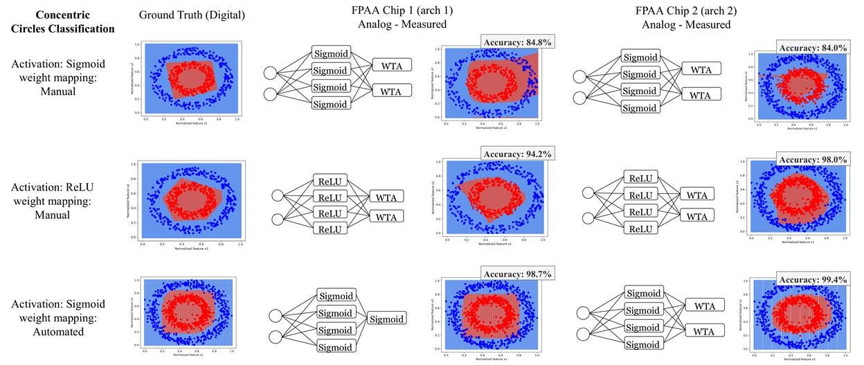
Figure 5: Small scale hardware validation of software framework on the concentric circles problem. Figure taken from this paper.
For the smaller scale hardware validation, they both implement a calibration flow for the FPAAs and develop a hardware aware offline training algorithm for the network. The circuitry and modeling have been designed to make use of programmability but to ensure the analog circuits actually follow the expected output they need to first be calibrated. There are two sources of mismatch that the calibration process is solving for, the first is inherent device mismatch from the foundry. The second is as a result of the indirect programming architecture on the FPAA. They perform this operation for over 100 devices, across 2 chips and across 50nA to 1uA currents. The results of the calibration shows that across all regions of operation they saw the FG accuracy increase the number of FETs within 1 standard deviation for at least 87% of the devices in the worst case. The approach for hardware aware training is to create a flow that takes an arbitrary problem with input features normalized to the range of the hardware and returns the weights and biases of an NN in its native analog parameters. Specifically, the target currents programmed to an FG. It is now feasible to integrate all parts of the multilayer perceptron on the FPAA. The problem chosen to validate the flow is the concentric circles classification problem, partly because it is a popular toy data set which can be visualized in two dimensions. Also, due to its simplicity for experimentation and complexity above linearly separable problems. The result of the automated weight mapping of the flow was a 98.7% and 99.4% hardware measured accuracy on the concentric circles problem with weights from the training loop.
Figure 6: Comparison of the energy consumption, accuracy of the digital and analog networks.
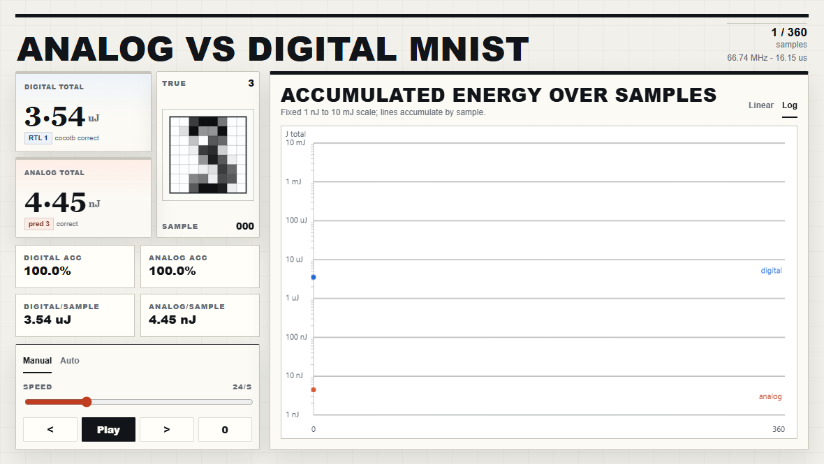
Finally, we scale up to MNIST on the analog side, and we put it on the same chart as the digital benchmark which allows us to see the ~1000x (3 orders of magnitude) energy improvement of the analog benchmark over the digital network. The video above shows a recording of an interactive dashboard that I had codex whip up. It compares the energy consumption of the digital baseline to the analog network across 360 validation samples. We also see the accuracy differences between the two approaches as it cycles through each sample. The chart is on a logarithmic scale to actually allow us to see both values on the same scale. For each sample in the top right of the control panel we see the ground truth value, the analog prediction and whether the cocotb index reported a correct/fail prediction.
As we wrap up, I do want to stress that similar to the point I made earlier about not ignoring the wisdom of previous analog designers, my overall goal is not to claim “digital is finished!” or anything silly like that. Rather, it’s to painstakingly acknowledge the beauty of the abstractions in other fields and show how this burgeoning field of analog computing can find ways to pull the best from these giants and demonstrate how much further we can go when we get closer to the physical world.